the Creative Commons Attribution 4.0 License.
the Creative Commons Attribution 4.0 License.
 | 05 Jul 2023
Development of a power station unit in a distributed hybrid acquisition system of seismic and electrical methods based on the narrowband Internet of Things (NB-IoT)
Feng Guo
Shenghui Liu
In this paper, we propose a new type of power station unit with wireless data transmission capability. This work breaks the limitation that conventional equipment is unable to upload data directly to a central unit. Based on that, a novel distributed geophysical data acquisition architecture is also proposed, enhancing the work efficiency by simplifying the system structure while maintaining core features. Designs that realise key functions including isolated high-power output, power management, wireless data transmission and high-precision clock synchronisation are introduced in this article. The prototype was packaged then, and a series of evaluation experiments were implemented to verify the key parameters of the instrument. Experiment results proved that the overall design of the instrument is feasible, and the key parameters outperform the industry leading instrument LAUL-428. Due to the wireless networking strategy, the proposed instrument further realises remote control and real-time data playback through the host computer software, making it suitable for joint geophysical exploration as well as microseismic monitoring. As for the system level, it could be customised by connecting different kinds of conventional acquisition stations for many kinds of prospecting targets.
- Article
(2362 KB) - Full-text XML
- BibTeX
- EndNote


The ambiguity problem of a single geophysical exploration method has always been a tricky problem in geophysical prospecting (Guo et al., 2020). Multi-method joint exploration has then become popular since it retains the advantages of different geophysical methods while reducing ambiguity problems. Among the different kinds of multi-method joint explorations, the joint exploration of seismic and electrical methods has become the research direction of many scholars (Garofalo et al., 2015; Wagner et al., 2019). However, the development of corresponding instruments is still at the very beginning.
Taking seismic exploration instruments as an example, the current seismometers can be divided into wired telemetry and wireless telemetry seismometers according to the communication method (Zhang et al., 2014). In the 1970s, Sercel had already launched the SN338 digital seismograph and corresponding single-channel acquisition station (Qiao et al., 2019); then they launched SN388, 408UL, 428XL, 508XT and other products successively. At present, the most advanced seismic acquisition system in the world is the 508XT system, which has a real-time acquisition capability. The 428XL seismic acquisition system, however, is the most widely used system in the entire geophysical prospecting industry at present, which has the most representative system arrangement structure. The system shown in Fig. 1a is mainly composed of a central control unit (e-428), a line control interface (LCI-428), a transverse station (LAUX-428), a line power (LAUL-428) and a collection chain (Link). The collection chain consists of several acquisition stations (FDU-428) or digital sensors (DSU-428) that are connected by cables (Sercel Inc., 2006). The LCI is the interface between the arrangement and the e-428 client, which plays a role in high-speed Ethernet routing. The main function of LAUX is to collect and package data from the arrangement and send them to another LAUX unit or the LCI. LAUL is connected directly with the Link through the cable; then power is supplied to the acquisition nodes on the Link and the data are relayed as well (Sercel Inc., 2007). The 508 system upgrades this structure further by combing LAUL and the LCI and replaces them with CX-508 (Sercel Inc., 2023). This, however, does not combine wireless communication functions (Duan, 2019). Besides, the Inova G3i NXT (Inova, 2022), I/O Scorpion (Gan, 2013) and seismic instruments (Dean et al., 2013) have the same system structure as 428XL, and a transverse station or line control interface is necessary. Other geophysical exploration systems, such as that for the multi-channel transient electromagnetic method (MTEM), have a similar structure in a cabled manner to the abovementioned system, and a wireless quality check function is added (Dong, 2015).
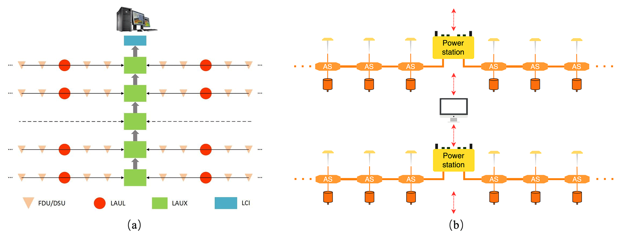
Figure 1(a) Structure diagram of the 428XL system; (b) system structure of the PSU (AS: acquisition station).
In spite of the increase in research, publishing and development on nodal seismographs, e.g. Hawk, SmartSolo, WTU-508 (Lv et al., 2022) and others developed by Tian (2020), the wired seismograph system is suitable for certain exploration situations (Ellis, 2014). As is found by Lansley (2012), the best exploration system structure in the near future should be a combination of wired and wireless systems, which could also be provided by the upgrade from the 428XL system to the 508XT system developed by an industry-leading company. In fact, as analysed by Dean et al. (2013), for dense exploration with a receiver interval of less than 40 m, the cabled system weighs less than the nodal system, and specifically, when the receiver interval is 10 m, the cabled system weighs only 24 % of the nodal system.
Combining the seismic and electrical acquisition stations developed by our team, a new type of power station unit (PSU) is proposed; thus a geophysical instrument networking method is also proposed in this article. The point is to retain the original functions of the LAUL and integrate the upward communication and human–computer interaction capabilities of the LCI by wireless communication. Therefore a 120-channel acquisition arrangement is developed based on a single PSU. This arrangement can be further expanded through wireless networking, which could be very convenient for joint geophysical exploration including seismic exploration and high-density electrical method exploration on complex terrain (Heath, 2008). Compared with traditional wired systems, the proposed structure can considerably reduce the amount of equipment needed to form an efficient work and data transmission flow.
The proposed PSU-based system is shown in Fig. 1b. A single PSU could connect and supply power to a series of acquisition stations (ASs) via the cable by two connectors, one on each side. The PSU serves as the main control unit by sending the control commands to the AS in a relay manner. After signal acquisition, the data are relayed on the line to upload from the AS at the end of the arrangement. The intermediate ASs add their own data to the data frame and then continue to upload forward until the PSU. Meanwhile, the PSU also acts as the human–computer interaction interface. Unlike the 428XL system, no cables or additional LCI are required between the PSU and the central control unit. Instead, wi-fi and narrowband Internet of Things (NB-IoT) are implemented as remote data transmission techniques, thus expanding the system scale to a larger extent through wireless networking. This layout is flexible and suitable for complex terrains in the wild or urban underground space detection.
2.1 Design targets
The design target is to integrate the functions that originally belonged to the LCI and LAUX into the PSU. Therefore, the aims are as follows:
-
solving the problem that the output voltage level of external battery decreases when discharging to provide stable and high-quality power to the acquisition station arrangement and monitoring the power status at the same time;
-
receiving control commands from the host computer and configuring the acquisition station arrangement accordingly while uploading received data to the host computer;
-
buffering and preprocessing the uninterrupted data stream uploaded by the acquisition stations;
-
providing a high-precision clock source for connected ASs and adding absolute time information to the data.
The PSU adopts a modular hardware design, consisting of an interface board, boost board (two pieces), power board, ARM® main control board (ARM® board), FPGA (field-programmable gate array) board, clock board and built-in back-up lithium battery. The hardware structure is shown in Fig. 2.
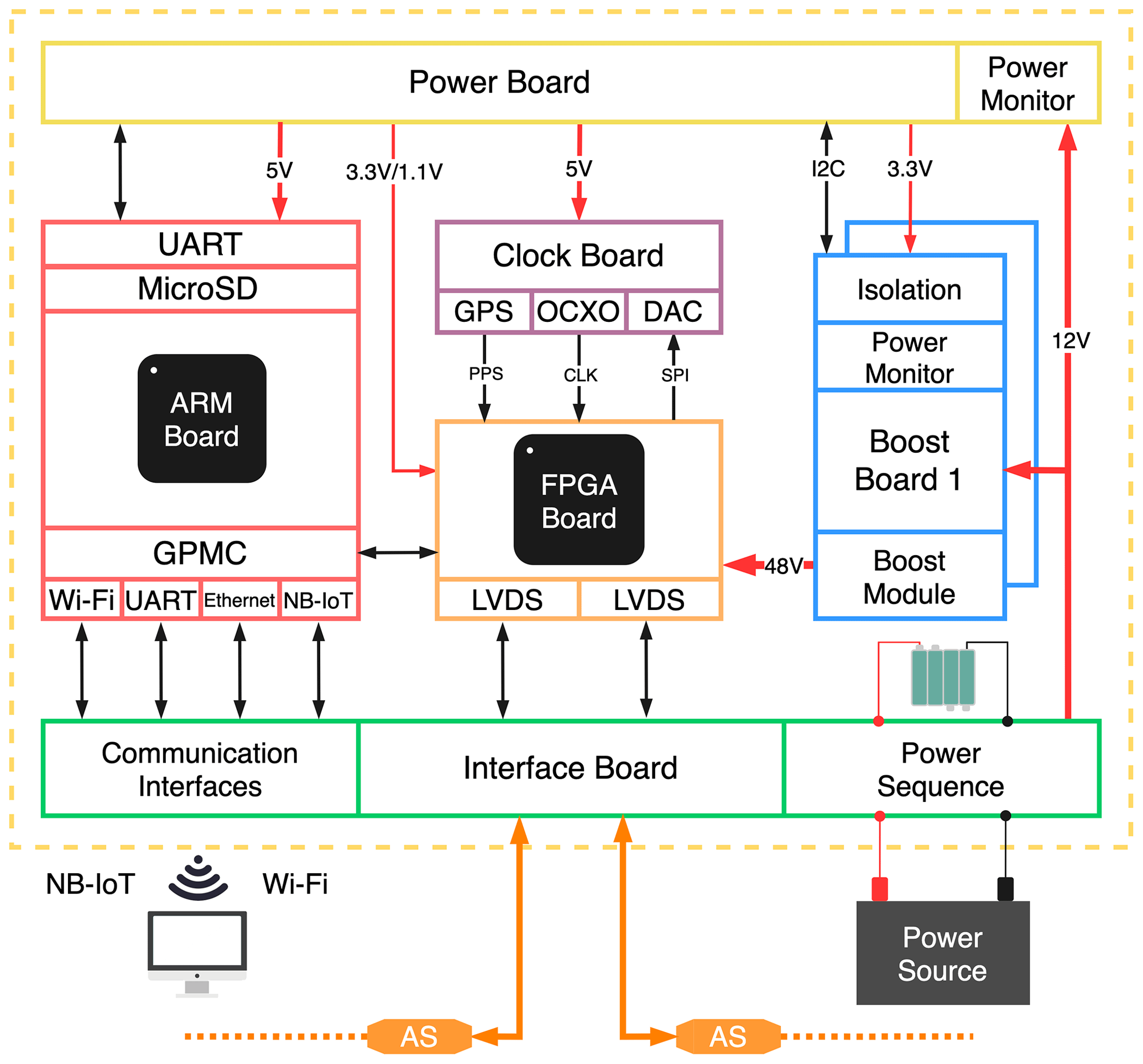
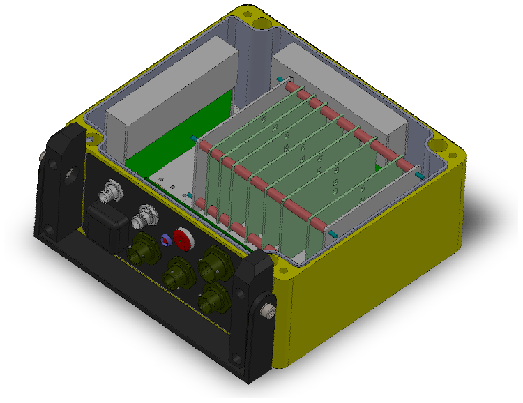
All circuit boards are fixed in the enclosure shown in Fig. 3. The interface board is installed on the connector side, and the other circuit boards are fixed together by metal screws on the bottom of the case. Between circuit boards, board-to-board connectors or flat cables are used. In this way, the spacing and quantity of the boards are adjustable; therefore the circuit boards could be replaced easily for fixing and upgrading.
3.1 Design of the interface board
The interface board mainly realises the transfer from each interface on the instrument enclosure to the internal circuits, whose shape and position therefore correspond to each interface on the enclosure.
Another main function of the interface board is to select a reliable power supply from the external battery or the built-in battery. In this case, the power path controller LTC4416 is introduced to control two sets of external P-channel metal oxide semiconductor field effect transistors (MOSFETs) to realise a nearly ideal diode function for the power switching circuit. It also expands the function of power sequencing while realising the power supply combination and reverse connection protection. When a valid external power supply is connected, the power source would be selected according to the preset voltage threshold, thereby saving the back-up battery. If the voltage level of the external source drops lower than that threshold, the back-up battery would be switched on to automatically avoid the power interruption due to external power failure during field exploration.
3.2 Design of the boost board
The function of the boost board is to output and monitor 48 V power, which is boosted from the unstable 12 V input from the external battery, for acquisition stations. To load more stations and provide flexibility during set-up, we designed a dual-output link strategy, which means two boost boards are needed for each power link.
3.2.1 Boost circuit
The voltage boost is realised by a VI-204-CX-type DC–DC (direct-current–direct-current) module, whose input voltage range is 10–20 V, and the output voltage is 48 V. In this case, our theoretical maximum output power is 75 W for a single boosted output source, and the conversion efficiency can reach up to 90 %. The power output of the PSU is controllable; therefore, the boost output can be turned off to reduce power consumption during parameter configuration when the power supply to the acquisition stations is not needed.
3.2.2 Output power monitoring circuit
In the PSU, the output power source is monitored by measuring current and voltage and simultaneously calculating the power value relying on LTC2945 utilising its integrated multiplier, which performs digital multiplication directly on the measured current and input voltage data to generate a 24 bit power value. Those acquired data are continuously sampled and stored in the internal register of LTC2945, and meanwhile the maximum and minimum values are updated (Linear Technology, 2012).
Both maximum and minimum thresholds for voltage, current and power can be configured. When a physical value beyond this threshold range is detected, a fault signal will be output through the ALERT pin. The microcontroller unit (MCU on the power board) configures this signal as an external interrupt source and will give a rapid response to this interrupt, which shuts down the 48 V output, in case abnormal situations happen.
3.3 Design of the power board
The main function of the power board is to monitor the input power and convert it to 5, 3.3 and 1.1 V power for other internal circuit boards. In addition, the control of the boost board, switches and LED indicators on the instrument panel is also realised by the power board.
3.3.1 Power board control circuit
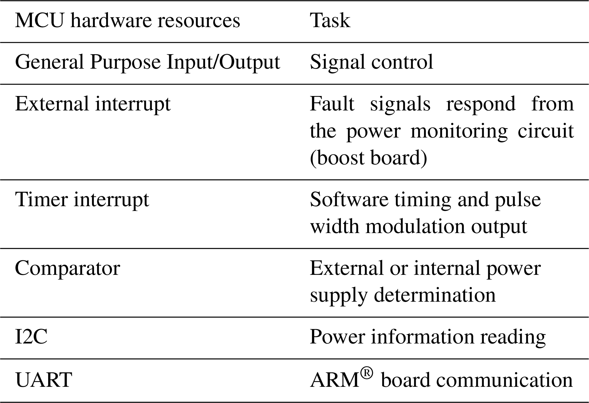
The main tasks of the power board control circuit are listed below; therefore an independent microcontroller is needed to achieve those complicated functions. Here, the MSP430G2553 is selected.
Table 1Power board control MCU task and hardware resources needed.
3.3.2 DC–DC conversion circuit
The DC–DC conversion circuit is used to convert the unstable input voltage, usually 9–16 V using lead batteries, to a stable 5 V, 3.3 V and 1.1 V voltage for specific internal power requirements. Considering the large conversion voltage drop, the PTH08080W switching mode power supply module is used since it has a conversion efficiency of 80 %–93 % in the entire load range, which is 4.5–18 V for input and 0.9–5.5 V for adjustable output.
3.4 Design of the ARM® main control board
The ARM® board integrates the core board of the AM4379 (Texas Instrument, 2013) processor and various communication interfaces. The structure of main control board is shown in Fig. 4.
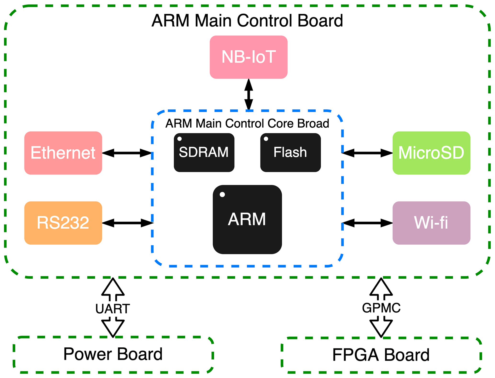
The ARM® board communicates with the FPGA using a general purpose memory controller (GPMC) interface and interacts with the power board through the UART (Universal Asynchronous Receiver/Transmitter) serial port. Acquisition data are stored on a microSD card. Remote monitoring and control are carried out through NB-IoT. In addition, a 2.4 and 5 GHz dual-band wi-fi module is introduced to realise wireless control and data transmission. For back-up data transmission and debugging interfaces, ethernet and RS232 serial ports are also reserved. In this case, an industrial-grade core board SOM-TL4379 based on TI AM4379 is used.
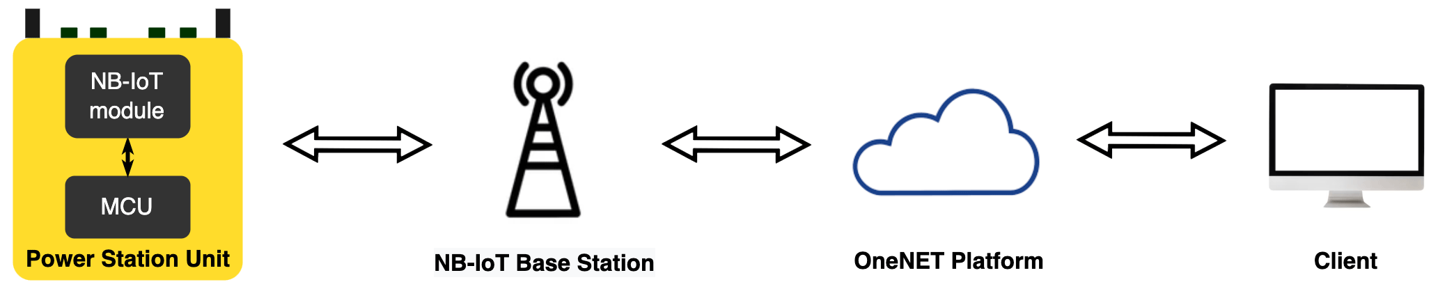
NB-IoT realises remote data transmission between the PSU and the upper computer at low power consumption. The NB-IoT chip called the M5310-A communication module supports LTE Cat-NB1/NB2 and has the characteristics of low power consumption (3 µA in power-saving mode, PSM) and an ultra-high operating temperature range. The network topology is shown in Fig. 5. Data are transmitted from the MCU through the UART interface to the NB-IoT module and then uploaded to the OneNET cloud platform via the NB-IoT base station (China Mobile, 2018). The client then accesses the uploaded data from the OneNET cloud platform.
Wi-fi, on the other hand, is introduced for high-speed wireless acquisition data uploading (to the upper computer) and other functions. In the proposed instrument, the TiWi5 wi-fi module supporting 2.4 and 5 GHz dual-frequency bands is used (Laired Connectivity, 2016). Compared to the 2.4 and 5 GHz frequency band relieves network congestion, providing better signal coverage and faster transmission speed.
3.5 Design of the FPGA board
The FPGA board is used to process a huge number of digital signals and logic control (De La Piedra et al., 2012). The main functions are as follows:
-
communicate with the acquisition stations based on the improved low-voltage differential signalling (LVDS) interface to achieve the acquisition station control and data uploading from acquisition stations to the PSU;
-
receive control commands from the ARM® board and transmit the acquired data to the ARM® board using the GPMC interface;
-
control the clock board and complete GPS signal analysis as well as oven-controlled crystal oscillator (OCXO) calibration.
LVDS communication is well supported by the FPGA 5CEBA2F7 with an integrated on-chip LVDS transceiver. OCT (on-chip termination) can be used by the LVDS receiver to achieve impedance matching, without external termination resistors.
The transmission signal on the line is a high-voltage signal based on Power over Ethernet (PoE) technology realising the power supply and data transmission simultaneously. This provides the explanation of the ARM® FPGA dual-core design. LVDS data in Manchester encoding from the cable are decoded by the FPGA and transmitted to the ARM® board for further data uploading, processing or internal data storage.
3.6 Design of the clock board
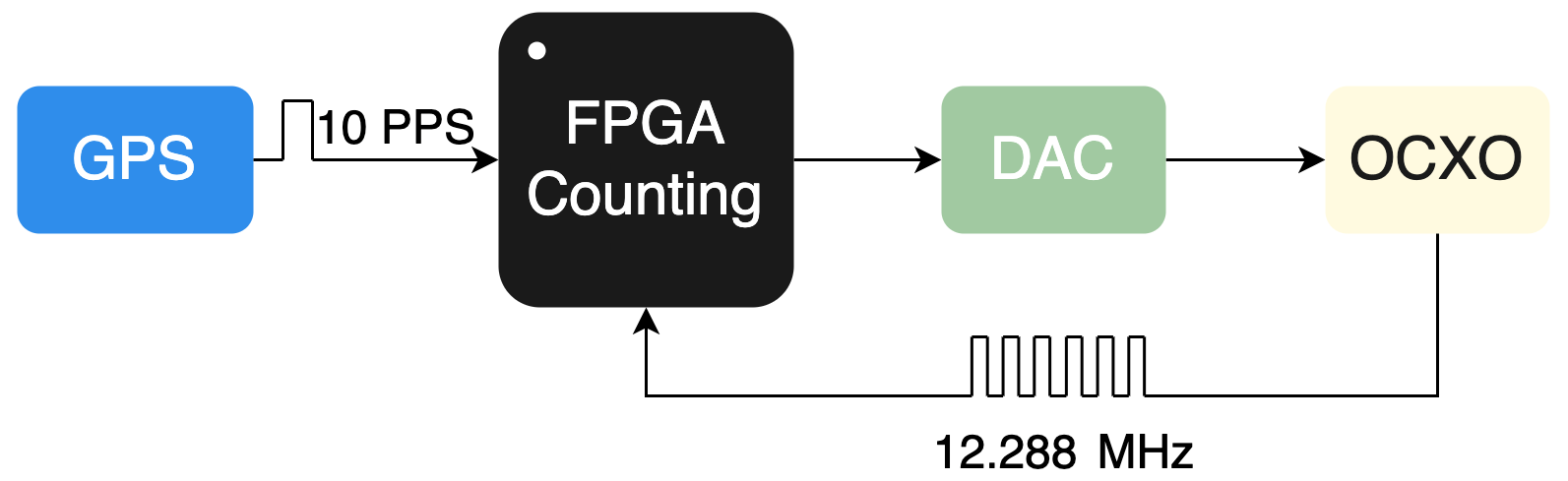
To improve the measurement accuracy of ASs and achieve synchronisation between PSUs, an accurate clock source is required (Cao et al., 2010). The high-precision clock system design scheme is shown in Fig. 6. The FPGA uses 10 accumulative pulse per second (PPS) signals generated by the GPS receiver as the time gate to measure the frequency of the OCXO. Frequency deviation of the OCXO is then calculated, and the corresponding calibration value is obtained. According to the calibration value, the digital voltage control value is generated and sent to the digital-to-analog converter (DAC). After conversion, the analog voltage is output to the voltage control terminal of the OCXO to realise the calibration.
The LEA-6T GPS module, whose timing accuracy reaches 15 ns, performing timing when only one satellite is visible, is utilised in this case (U-blox, 2017) to ensure the precision of the PPS source.
The OCXO on the other hand reduces the output frequency change in oscillator caused by temperature variation by stabilising the internal temperature, but there is still cumulative error. As the working time increases, the clock error will gradually increase. Take the OCXO in this case as an example, whose output frequency is 12.288 MHz with a frequency stability of . If no calibration is implemented, the accumulated error after 1 d could be
Here, fs is the standard frequency of the OCXO and k represents the frequency stability.
Assuming that the sampling interval is set to 1 ms, there will be an error of four sampling points after a 1 d acquisition. Therefore, the OCXO must be calibrated to improve the frequency accuracy.
The selected OCXO is voltage controlled; thus a voltage of 0–5 V is applied to the CONTROL pin to achieve precise adjustment of the output frequency, and the pull range is s. The 12 bit DAC7512 (Texas Instrument, 2012) is used to produce the control voltage, producing the frequency adjustment of s per step. Since then, accurate frequency calibration could be achieved.
The software integrated into this proposed instrument is mainly composed of the power board software, ARM board software and FPGA board software. The reason for this separated software design is to give full play to the advantages of different CPUs to achieve the predetermined functions. For example, the power board software can provide power management for the whole instrument when the acquisition station is not turned on so as to ensure the normal startup of the instrument system. The software on the FPGA board uses FPGA to implement multi-channel parallel data acquisition and clock calibration.
4.1 Power board programming
The power board mainly realises the functions of power monitoring, including fault response, boost board control and interface board control. The program flow chart is shown in Fig. 7.
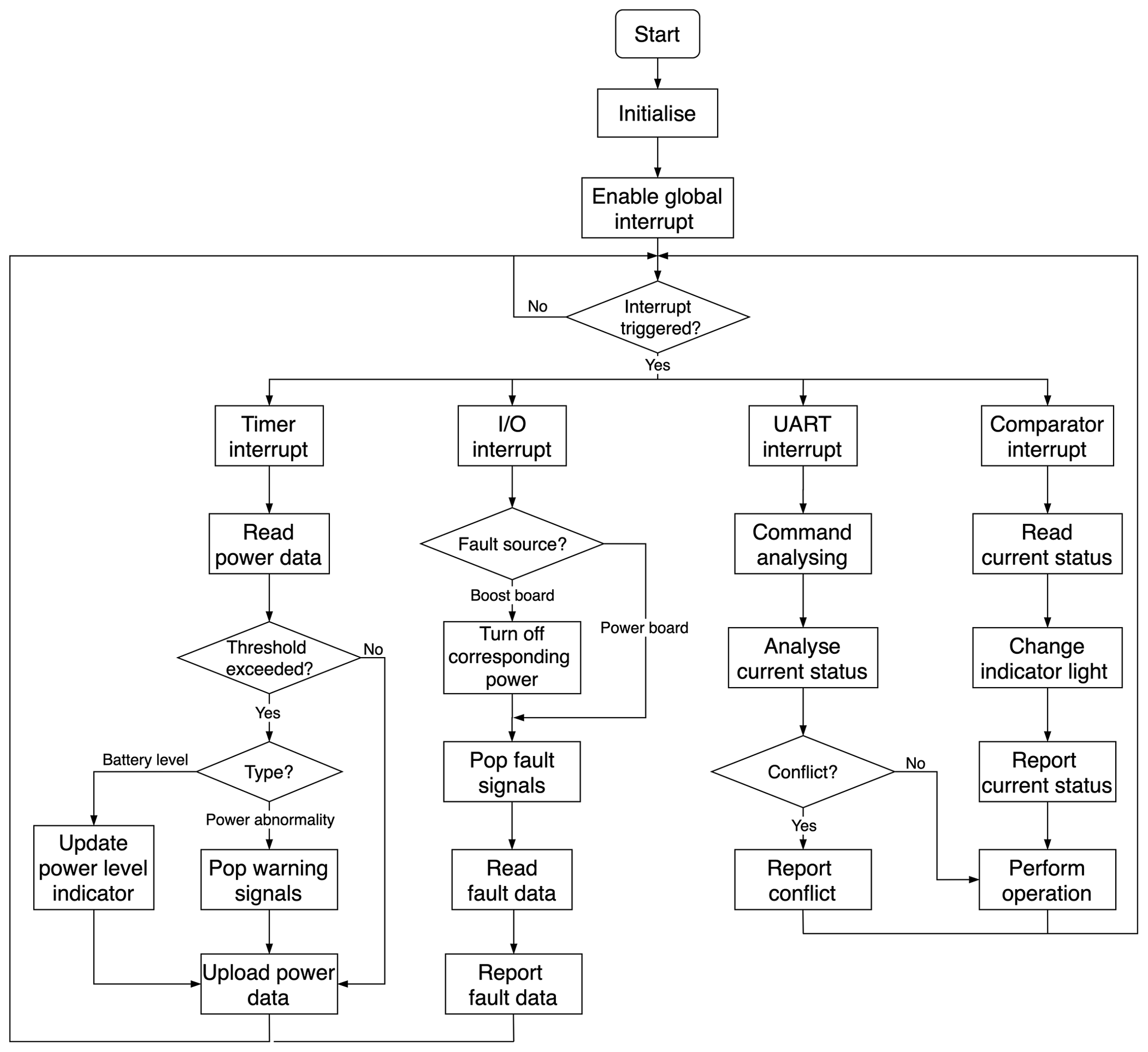
After the MCU on the power board is powered on, modules including GPIO, timer, serial port, comparator and I2C interface will be initialised first. Then, the global interrupt is turned on, while the MCU enters the low-power-consumption mode, and it will not be awakened until the interrupt is generated.
The timer interrupt interval is set to examine the power source status. When the timer interrupt request is generated, the MCU will read the data in the register of LTC2945. If the threshold value is not exceeded, the data will be uploaded directly to the ARM® board in a specific format, and the MCU sleeps again to enter the low-power-consumption mode. If there is a certain item of data that exceeds the threshold, further judgement will be carried out to analyse the type of data that exceeds the threshold. When the battery voltage drops to a certain segment point, the status of the battery indicator will be switched on. If the output voltage, current or system power exceeds the normal operating range, an early warning signal will be issued to prompt the user to troubleshoot.
There are three interrupt sources for I/O interrupts, connecting to the “Alert” signals of three pieces of LTC2945 respectively. If the fault comes from the boost board, the MCU will shut down the corresponding boost module first to ensure the safety of the acquisition line and then send a fault signal through the indicator light to remind the user and upload the fault data to the ARM® main control board. If the fault comes from the battery that inputs power, since the power switch cannot be turned off directly by the software, the MCU can only issue a fault indication and upload fault data.
The serial port of the MCU is connected to the ARM® board, and the serial port interrupt is used to respond to the control commands of the ARM® board. After receiving the serial port data, the MCU will parse out the command and determine whether it conflicts with the current state. If there is no conflict, the corresponding operation will be executed directly. However, on condition that a conflict exists, meaning that there is a communication problem between the power board and the ARM® main control board, the conflict will be reported to the ARM® board.
The power selection indication signal output by LTC4416 is connected to the comparator input port of the MCU. When the power supply is switched between the external power supply and the back-up battery, the comparator interrupt is triggered. Then the MCU will determine the current power source and report the status to the ARM® board.
4.2 ARM® application programming
As the main control unit of the PSU, the ARM® board needs to receive commands from a host computer to complete tasks including power supply management, parameter settings, and storing and uploading data. The number of data to process is huge and multiple tasks are executed concurrently. Therefore, an operating system must be equipped to manage system resources and schedule multiple applications uniformly and to provide users with file systems and hardware access interfaces.
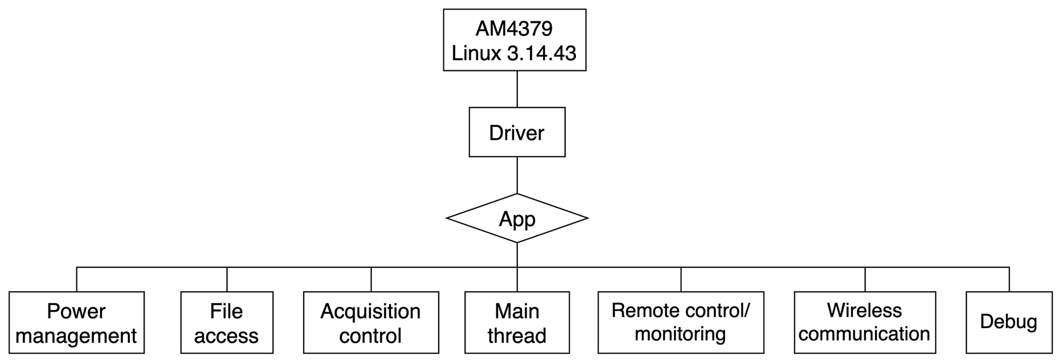
The ARM® board applications are developed based on the Linux platform and details are given in Fig. 8. The main tasks are (1) communicating with the power board to manage the PSU and the acquisition station arrangement; (2) accessing the microSD card for file access; (3) communicating with the FPGA board to control the acquisition stations and to receive acquired data from the acquisition stations; (4) accessing the wi-fi module to realise the wireless communication function; (5) communicating with the NB-IoT module through the serial port to realise remote control and real-time quality monitoring; and(6) debugging through the serial port and network port.
Each part of the function is implemented by a separate thread to improve the response speed of the application and ensure that the system is not blocked by a task occupying too much time. In addition, there is a main thread module, running after the system is launched, which is mainly responsible for device initialisation and starting other threads.
4.3 Design of the FPGA board program
4.3.1 Manchester encoding
The high-speed data transmission between the PSU and AS is based on improved LVDS, and the PoE power supply as well as signal isolation are realised through the isolation transformer. But at the same time, the isolation transformer will also cut off the DC component of the signal. Therefore, only the AC component of the input signal will be observed at the receiver. When continuous binary 0 or 1 appears in the data, the voltage at the receiving end will drop, causing signal jitter and bit errors. Therefore, the Manchester encoding technology is introduced to solve this problem. The positive edge represents data 0, and the negative edge represents data 1 (Lalitha and Kathiravan, 2014; Suchitra, 2013). However, since 2 bits of data are used to represent 1 bit of information, the data transmission efficiency is reduced by half.
4.3.2 Design of the clock board control program
The frequency measurement calibration program is implemented by the FPGA using an HDL (hardware description language), which is mainly composed of the delay reset module, the clock calibration module and the DAC control module. The program workflow is illustrated in Fig. 6. The delay reset module releases a reset signal 10 s after power-on to wait for the internal oven-controlled chamber of the OCXO reach the working temperature. The clock calibration module then measures the output frequency of the OCXO while calculating the calibration amount. The gate time used for measurement is the time interval of 11 consecutive PPS signals (10 s). Within the gate time, the output of the OCXO is counted and compared with the theoretical value to generate a calibration value, which is output to the DAC control module. The DAC control module then generates the control signal and writes it in a certain timing sequence to DAC7512. In this way, a single calibration is executed. When the difference between the counted value and the theoretical value decreases to a certain range, the calibration is completed.
After the design and assembly of the instrument, a series of verification experiments were implemented to evaluate the major performance of the instrument.
5.1 Output power experiment
Supplying power to the acquisition line on both sides is the key function of the power station unit; thus the load capability of the PSU is an important technical parameter. Firstly, a simulated load is used instead of ASs to evaluate the maximum power output ability. The average measured output power of one side is
According to the results above, the total load capacity of the power station unit can reach 131.66 W.
We then implemented an output power evaluation experiment with ASs to illustrate the output power variation with different AS quantities. Acquisition stations of one seismic and one electrical acquisition channel have been chosen as the load, and the interval between acquisition stations is 20 m in the experiment. Both power output ports are used to decrease the power consumption on the cable. The output curve with AS quantity increasing is illustrated in Fig. 9, which was fitted from seven sets of discrete output power value points listed in the table in the upper left corner. This experiment proved that the proposed PSU could supply power to 120 ASs.
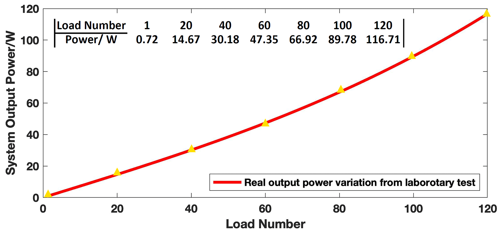
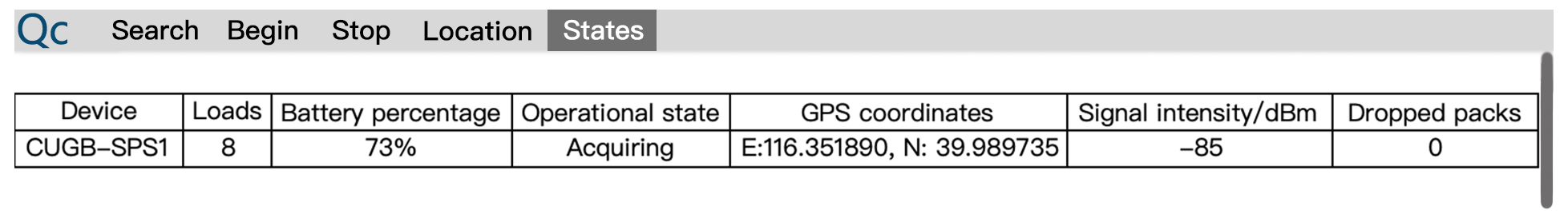
Figure 10NB-IoT remote-control interface.
5.2 Remote-control experiment
To upload quality control information and realise the human–computer interaction, a communication experiment based on NB-IoT is carried out to achieve the data transmission from end to cloud. As is shown in Fig. 10, the remote-control functions include online device scanning, acquisition status control, battery status, GPS information and network signal strength. In the evaluation experiment, the PSU supplied power to eight seismic–electrical hybrid acquisition stations simultaneously, and the acquisition stations are controlled to enter several working conditions through remote commands. Other indoor performance experiments have been implemented as well, and the result shows that the downstream data throughput is 8.86 kbps (kilobits per second) on average and the package latency is 1183 ms based on the LWM2M protocol. By remote controlling, long-term monitoring during joint prospecting of seismic and electrical methods can be carried out, and it has good application prospects in urban underground space detection and shallow surface wave exploration. Using the NB-IoT network can avoid serious interference from the wireless network, providing better signal coverage and signal quality.
5.3 Comparison
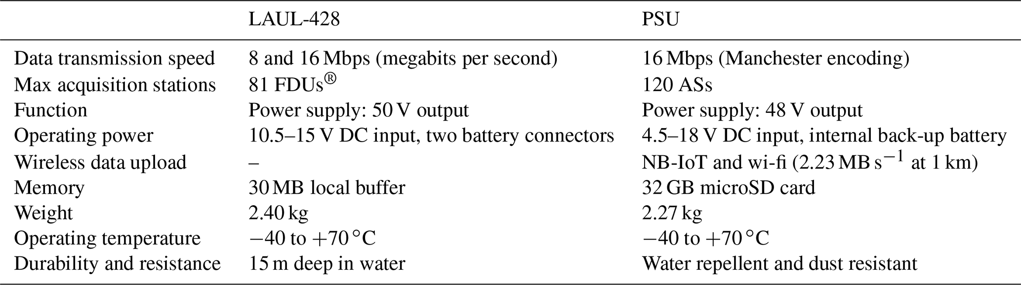
After the abovementioned evaluation experiments, comparison between the proposed PSU and the state-of-the-art LAUL-428 is listed in Table 2. First, the proposed PSU has an advantage in providing power to more acquisition stations (ASs) simultaneously than LAUL-428. The test is carried out under the condition of a 20 m interval between each AS with a 2 ms sampling interval to match the test condition of LAUL-428 provided by Sercel's official manual (Sercel Inc., 2007). Another technical advantage is that the PSU has the ability of data communication, which is not supported by LAUL-428.
In this article, a new power station unit is designed for joint geophysical exploration. Combining hybrid acquisition stations and upper-computer software, a novel distributed wireless seismic- and electrical-method, hybrid acquisition system becomes realistic as well.
Compared with the traditional wired seismograph system, the structure of the PSU system is much simpler, and the acquisition data could be uploaded directly from the PSU to the central unit through a wireless local area network.
The proposal of a PSU system has several advantages over nodal instruments as well (Qiao et al., 2019). Firstly, power supply through the proposed PSU could be more stable and sustainable and is more convenient for power management. Secondly, unlike the nodal instrument, which uploads data individually, the PSU packs data from 120 acquisition stations and upload them to the central unit through a WLAN in real time, therefore alleviating the channel congestion problem and providing a long-term stable work support and a larger channel quantity. Owing to the NB-IoT technology, which provides the functions of remote control and quality check, networking with other IoT-based instruments for multi-parameter geophysical exploration could be expected.
The PSU simplifies the system structure of seismic and electrical prospecting and reduces the overall cost, forming a wired and wireless hybrid distributed acquisition system. A multitude of geophysical exploration methods, namely reflection, refraction, surface wave exploration and high-density electrical exploration could be carried out. In conclusion, the proposed PSU is a crucial part of a new distributed hybrid acquisition system architecture of seismic and electrical prospecting.
No data sets were used in this article.
FG: writing (original draft), review and editing, software. QZ: conceptualisation, funding acquisition, supervision. SL: hardware design and validation.
The contact author has declared that none of the authors has any competing interests.
Publisher’s note: Copernicus Publications remains neutral with regard to jurisdictional claims in published maps and institutional affiliations.
This work has been supported by the Natural Science Foundation of China, the PetroChina Innovation Foundation, and the National Key Research and Development Program of China.
This research has been supported by the Natural Science Foundation of China (grant nos. 42074155, 41574131 and 41204135), the PetroChina Innovation Foundation (grant no. 2019D-5007-0302), and the National Key Research and Development Program of China (grant nos. 2022YFF0706202 and 2021YFC2801404)
This paper was edited by Alessandro Fedeli and reviewed by three anonymous referees.
Cao, P., Song, K., Yang, J., and Ruan, F.: Design of a large remote seismic exploration data acquisition system, with the architecture of a distributed storage area network, J. Geophys. Eng., 8, 27–34, https://doi.org/10.1088/1742-2132/8/1/005, 2010.
China Mobile: M5310-A NB-IoT communication module, http://iot.10086.cn/Uploads/file/product/20181109/M5310-A_20181109103230_35807.pdf (last access: 9 December 2022), 2018.
Dean, T., O'Connell, K., and Quigley, J.: A review of nodal land seismic acquisition systems, Preview, 164, 34–39, https://doi.org/10.1071/pvv2013n164p34, 2013.
De La Piedra, A., Braeken, A., and Touhafi, A.: Sensor systems based on FPGAs and their applications: A survey, Sensors, 12, 12235–12264, https://doi.org/10.3390/s120912235, 2012.
Dong, Q. Y.: Implementation of battery management unit in MTEM system, MS thesis, University of Science and Technology of China, China, 71 pp., https://kns.cnki.net/KCMS/detail/detail.aspx?filename=1015589943.nh&dbname=CMFDTEMP (last access: 10 Feburary 2023), 2015.
Duan, C. P., Zhai, L. X., Wu, S. P., Liu, P., and Jian, Y.: Function description and application of CX-508 in seismic data acquisition system, Equip. Geophys. Prosp., 29, 80–83, 2019 (in Chinese).
Ellis, R.: Current cabled and cable-free seismic acquisition systems each have their own advantages and disadvantages – is it possible to combine the two?, First Break, 32, 91–96, https://doi.org/10.3997/1365-2397.32.1.72599, 2014.
Heath, R. G. : Trends in land seismic instrumentation, The Leading Edge, 27, 872–877, https://doi.org/10.1190/1.2954026, 2008.
Gan, Z. Q.: Discussion on performance analysis of several mainstream seismic exploration instruments, Petroleum Instruments, 27, 21–24, 2013 (in Chinese).
Guo, F., Zhang, Q., Zhang, Q., Li, W., Luo, Y., Niu, Y., and Qiao, S.: Development of a new centralized data acquisition system for seismic exploration, Geosci. Instrum. Method. Data Syst., 9, 255–266, https://doi.org/10.5194/gi-9-255-2020, 2020.
Garofalo, F., Sauvin, G., Socco, L. V., and Lecomte, I.: Joint inversion of seismic and electric data applied to 2D mediaseismic and electric data joint inversion, Geophysics, 80, 93–104, 2015.
Inova: G3i NXT: https://d1cvtcw7p7ix4u.cloudfront.net/images2/downloads/G3i-NXT-Datasheet_yellowlogo.pdf?mtime=20220404153431&focal=none, last access: 9 December 2022.
Laired Connectivity: TiWi5 dual-mode Wi-Fi module with Bluetooth: https://www.lairdconnect.com/wireless-modules/wifi-modules-bluetooth/tiwi5-dual-mode-wifi-module-bluetooth (last access: 9 December 2022), 2016.
Lalitha, V. and Kathiravan, S.: A review of manchester, miller, and fm0 encoding techniques, SmartCR, 4, 481–490, 2014.
Lansley, M.: Cabled versus cable-less acquisition: making the best of both worlds in difficult operational environments, First Break, 30, 97–102, 2012.
Linear Technology: LTC2945 – Wide range I2C power monitor: https://www.analog.com/media/en/technical-documentation/data-sheets/2945fb.pdf (last access: 9 December 2022), 2012.
Lv, S., Lin, J., Yang, H., Tian, R., Wang, L., Bin, K., Tong, X., and Li, A.: Development and prospect of the nodal cable-free seismograph: a review, Meas. Sci. Technol., 33, 102001, https://doi.org/10.1088/1361-6501/ac72fa, 2022.
Qiao, S. Q., Zhang, Q. S., and Zhang, Q. M.: Mine fracturing monitoring analysis based on high-precision distributed wireless microseismic acquisition station, IEEE Access, 7, 147215–147223, https://doi.org/10.1109/ACCESS.2019.2946443, 2019.
Sercel Inc.: 428XL reference training guide, Carquefou Cedes France: Sercel Inc, 2006.
Sercel Inc.: 428XL user manual, Carquefou Cedes France: Sercel Inc, 2007.
Sercel Inc. 508XT Brochure: https://www.sercel.com/products/Pages/508-XT.aspx/, last access: 31 January 2023.
Suchitra, S.: Vhdl Implementation of Manchester Encoder and Decoder, International Journal of Electrical, Electronics and Data Communication, 1, 2320–2084, 2013.
Texas Instrument: Low-power, rail-to-rail output, 12-bit serial input digital-to-analog converter, https://www.ti.com/lit/ds/symlink/dac7512.pdf?ts=1599707710212&ref_url=https%253A%252F%252Fwww.ti.com%252Fsitesearch%252Fdocs%252Funiversalsearch.tsp%253FsearchTerm%225DDAC7512 (last access: 9 December 2022), 2012.
Texas Instrument: MSP430G2X53 mixed signal microcontroller, https://www.ti.com/lit/ds/symlink/msp430g2553.pdf?ts=1599736963866&ref_url=https%3A%252F%252Fwww.ti.com%252Fsitesearch%252Fdocs%252Funiversalsearch.tsp%253FsearchTerm%253Dmsp430g2553 (last access: 9 December 2022), 2013.
Tian, R. Y., Wang, L. X., Jiang, Y. J., Lin, J., Zhang, L. H., and Zhou, X. H.: Wireless Multi-Hop Energy-Efficient System for High-Density Seismic Array, IEEE Access, 8, 26054–26066, https://doi.org/10.1109/ACCESS.2020.2971083, 2020.
U-blox: LEA-6 u-blox 6 GPS Modules Data Sheet: https://content.u-blox.com/sites/default/files/products/documents/LEA-6_DataSheet_(UBX-14044797).pdf (last access: 7 June 2023), 2017.
Wagner, F. M., Mollaret, C., Günther, T., Kemna, A., and Hauck, C.: Quantitative imaging of water, ice and air in permafrost systems through petrophysical joint inversion of seismic refraction and electrical resistivity data, Geophys. J. Int., 219, 1866–1875, https://doi.org/10.1093/gji/ggz402, 2019.
Zhang, S., Zhang, L., Lin, J., and Sun, F.: Summary of development of telemetry seismometers, Prog. Geophys., 29, 1463–1471, 2014 (in Chinese).